技术资料
白皮书和应用说明
Stress State Determination in Nanoelectronic Silicon Devices Coupling COMSOL Multiphysics and a Recursive Dynamical CBED Pattern Simulation
发布日期 2008
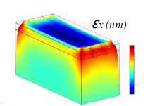
Strained technology is being promoted as the best way to extend the performance of semiconductor transistors. An inhomogeneous layer deposited on top of a silicon device can induce a strong modification in the real silicon strain state, and consequently in its electronic performance. Coupling the finite elements analysis done by COMSOL with a recursive CBED and LACBED dynamical simulation, we are able to explain the observed diffraction pattern modification, reconstructing the strain field in the device.
下载
- Spessot_pres.pdf - 4.77MB
- Spessot.pdf - 0.67MB