Simulation of Nonlinear Optical Absorption in Silicon Optical Waveguide
From the perspective of nonlinear silicon photonics, the strong light confinement in sub-micron sized silicon waveguides increases the effective nonlinearity. However, the high optical power density in the waveguide core also increase nonlinear absorption and hence the device self-heating [1]. In this work, effects of two photon absorption (TPA) and TPA-induced free carrier absorption (FCA) are investigated at the 1550nm telecom wavelength (C-band) in continuous-wave light scenario.
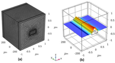
In the first part of the work, beam envelope method in wave optics module is implemented for a 3D nonlinear silicon waveguide optical transmission simulation. The first principle nonlinear loss definition is introduced to the imaginary part of silicon refractive index, which is a function of the spatial electric field strength. Buffer regions with linear silicon refractive index are used to facilitate boundary optical mode computations. As shown in Fig.1, it is feasible to simulation a first principle 3D nonlinear optical transmission through a 0.5mm long silicon waveguide. Linear discretization is used to make this 3D simulation run possible on a laptop with 8GB free memory. Given adequate computational resources, the coupled TPA-induced free carrier effects and self-heating in silicon may be simulated in full dimension.
In the second part of the work, an approximated 2D+1D segmented model (2D cross section and 1D propagation direction) has been used to downscale the overall computational cost and time. And a computationally lite application is built for web-based Comsol server usage scenario. The two-dimensional opto-thermal simulations are shown in Fig.2. Wave optics module is used to simulate the optical waveguiding mode in the 2D cross section of waveguide. Optical energy density (correlated to optical power flux density) are used to approximate first principle nonlinear optical absorption (TPA and FCA) with the relevant effective area value. Here all absorbed light power density (in unit of W/m3) are assumed as spatial heating source in the core of silicon waveguide. Heat transfer module is used to simulate the thermal problem in this 2D cross section of waveguide. For realistic estimation of silicon-on-insulator structure, the thermal problem considers stacks of a 500um-height silicon substrate and a 2um-height silicon dioxide layer. A realistic heat transfer coefficient is defined at the bottom of silicon substrate to emulate cooling effects by a heat sink. One-dimensional opto-thermal simulation are shown in Fig.3. Two-dimensional solutions from optical and thermal solvers (shown in Fig.2) are projected into parameters used in a 1D effective propagation equation of optical power along waveguide propagation direction, which is implemented in general PDE form. The approximated temperature rise is interpolated as function of optical power based on pre-calculated 2D solution.
References 1. Minhao Pu, Yaohui Chen, Kresten Yvind, Influence of thermal effects induced by nonlinear absorption on four-wave mixing in silicon waveguides, IEEE conference on Group IV photonics, 2014.
下载
- COMSOL_conf2020_poster_yaohuic.pdf - 0.74MB