Using the Schrödinger Equation Interface
Part 4 of this semiconductor modeling course begins with an introduction to the Schrödinger Equation interface and how it can be used to solve the single-particle Schrödinger equation for a wave function. We will also talk about how the Schrödinger Equation interface can be used in conjunction with the Electrostatics interface via the Schrödinger-Poisson multiphysics coupling,
Discussion: Schrödinger Equation Interface
Here, we take a look at the Schrödinger Equation interface that is available within the Semiconductor Module. This is used to solve the single-particle Schrödinger equation in 1D, 2D or 3D. Using this interface, you will be able to solve for eigenenergies of bound states, decay rate of quasibound states, transmission and reflection coefficients and effective band structure of superlattice. We also go over how and when to use the Schrödinger-Poisson multiphysics coupling.
Demo: Double Barrier
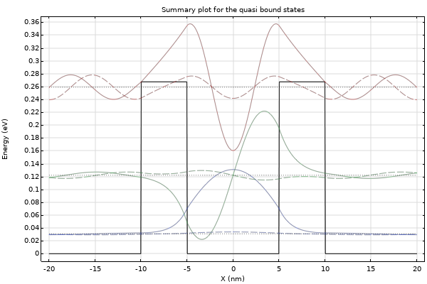
Below, we demonstrate an envelope approximation using the 1D Double Barrier tutorial model to solve for the wave functions and energies for quasibound states and the reflection and transmission coefficients versus energy. The model uses the envelope function approximation and is assumed to be constructed from layers of gallium arsenide (GaAs) and Aluminum Gallium Arsenide (AlGaAs). With this, you will see the model-building process from start to finish.
Demo: Silicon Inversion Layer
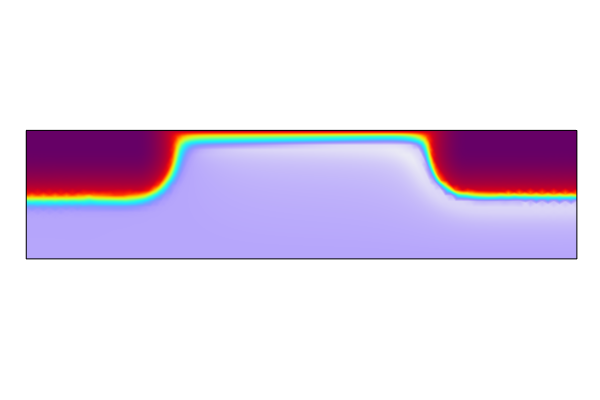
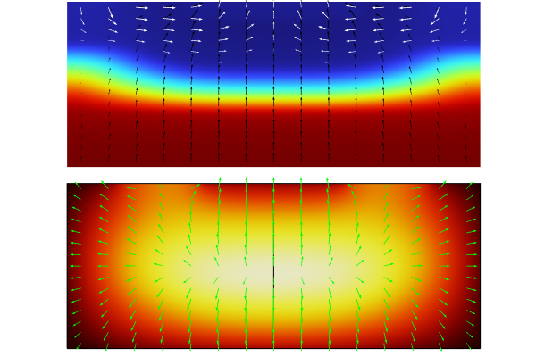
As semiconductor technology continues to produce smaller and smaller devices, the effects of quantum confinement become increasingly important. With the Silicon Inversion Layer tutorial model, you will be able to compare the Density Gradient and Schrödinger-Poisson methods while taking quantum effects into account. In this video, we will introduce the model and talk you through the basic features you will need to complete this exercise.
请提交与此页面相关的反馈,或点击此处联系技术支持。

