Coupling Picosecond Terahertz Pulses to a Scanning Tunneling Microscope
Probing ultrafast processes over subpicosecond and picosecond time scales provides fundamental insight into the nature of materials. We have experimentally demonstrated terahertz (THz)-pulse-induced tunneling in a scanning tunneling microscope (THz-STM) to image surfaces with simultaneous nanometer spatial resolution and subpicosecond time resolution [1]. However, the exact mechanism by which THz radiation couples to the scanning probe tip of the STM is not completely understood. THz radiation can excite surface plasmon polaritons (SPPs), which propagate as Sommerfeld waves along a metal wire waveguide with low loss and dispersion[2,3]. For metal wires with a sharp taper, electromagnetic fields are enhanced due to the localization of SPPs at the apex[4,5].
In this study, we investigate the coupling of THz pulses to a STM tip above a sample via finite-element time-domain simulations in a 3D model of the THz-STM geometry (Figure 1). In this simulation created in COMSOL Multiphysics® software, the model is only focused on the tip-sample region that is illuminated by THz radiation. The modeling domains are strategically meshed so that the mesh sizes around the tip apex are nm-sized and the outer domain mesh sizes are a fraction of the THz wavelength (100 µm). The Wave Optics Module is employed, where a THz pulse with picosecond pulse duration and spectral power peaked at 0.5 THz, electric field peak amplitude of 20,000 V/m, and a spatial Gaussian beam width of 1.9 mm, is excited at a port and propagates towards the tip-sample junction. The domains representing the tip, tip holder and sample are conducting regions that are assigned nominal Drude conductivity values at 0.5 THz. Probes are placed at the port and below the tip apex to measure the electric field components generated by the solver. In this simulated experiment, the tip-sample distance, angle of incidence[6], the polarization of the pulse and the tip geometry can be varied.
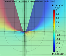
The propagation of the THz pulse from the port to the tip-sample junction, the focusing of the pulse around the tip apex and the scattering of THz radiation are animated (Figure 2). In the simulation, scattering, waveguide propagation (Figure 3) and near-field enhancement (Figure 4) are observed. The near-field radiation (Figure 4) resembles plasmonic modes [3,7] in the regions surrounding the tip apex. The peak of the electric field at the tip apex is found to be about 4 orders of magnitude higher than the incident peak field (Figure 4b) for a 10 nm tip-sample separation.
In future simulations, defects and nanostructures will be introduced to the tip and sample geometry in order to investigate THz coupling efficiency and propagation of surface plasmons created at the tip-sample boundaries. The tip-sample junction may act as a THz antenna[8] where the geometry of the system has an important role in the frequency dependence of the THz coupling. The THz bias modulation at the STM tunnel junction can be explored with these simulations, which is crucial for understanding how THz-STM can probe ultrafast dynamics in materials on the nanoscale.
This work was supported by NSERC, AITF and iCiNano.

下载
- nguyen_abstract.pdf - 0.61MB


