Design of a Surface Plasmon Resonance Based S-R Latch Circuit
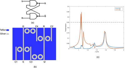
Surface plasmon polaritons are electromagnetic modes excited at the conducting-dielectric interface owing to the resonant interaction between incident photons and free electrons at the conducting surface. Plasmonic resonances confine optical power at subwavelength scales, which allows the miniaturization of optical devices and circuits beyond the diffraction limit. Many researches have been dedicated over the last two decades to optimize nanostructured waveguides and cavities for transmission and processing of optical signals at levels of integration comparable to electronic circuits. Recently, Abdulnabi and Abbas [1] proposed basic plasmonic logic gates made of an arrangement of silver nanoribbons and resonant rings on Teflon substrate. We extend this approach to design a surface plasmon resonance based S-R latch, a sequential circuit that can be applied as a one-bit memory device. In the figure below, we depict the schematic configuration of the circuit together with the corresponding plasmonic waveguiding structure for its implementation. The circuit has two inputs (one for setting (S) and other for resetting (R)) and two complementary outputs (Q and Q’). When S and R are excited with a plasmonic mode, with means that both receive a bit 1, the state of the outputs does not change. If S is changed to 0, then Q = 1 and Q’ = 0. On the other hand, Q = Q’ = 0 if only R is changed to 0. The output setup is not determined for S = R = 0. In the plasmonic waveguide, the terminals C1, C2, C3 and C4 are control ports that enable the operation of the circuit. The 2D Wave Optics Module with EWFD (Electromagnetic Waves, Frequency Domain) interface of COMSOL Multiphysics® was applied for the modeling of the circuit. The parametric sweep in the frequency domain study is implemented to compute the S-parameters for the wavelength range [800 nm, 2000 nm]. Continuity periodic conditions are applied at the boundaries of the circuit with corresponding periodic ports at specified inputs and outputs for the computation of the S-parameters. The transmission response is regarded as the squared magnitude of the S-parameter between a specified input-output pair. Since plasmonic excitations are TM modes, we set the model for in-plane electric field vector configuration in EWFD settings. The transmission spectrum for Q and Q’ for S = 0 and R = 1 is shown in the figure below as an example of the operation of the proposed all-optical S-R latch. The control ports are set up as: C1 = C2 = C4 = 1 and C3 = 0. The dashed line indicates the transmission threshold used to distinct between bit 1 (above 0.25) and 0 (below 0.25). Seminal simulation results suggest that the structure is promising to operate indeed as a optical version of a S-R latch.


