Device-Level Equivalence and Consistency of Interfacial Dipoles
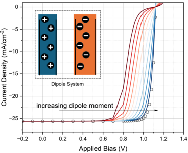
Interfacial dipoles are commonly represented in semiconductor device models by effective work-function or energy-level shifts. [1,2] However, whether such a reduced description remains equivalent to a spatially resolved dipole under device operating conditions is not obvious. Here, we investigate this question using a one-dimensional drift–diffusion model of a double-heterojunction solar cell consisting of a hole transport layer, absorber, and electron transport layer (ETL). The simulations were performed in COMSOL Multiphysics® 6.2. The interfacial dipole was explicitly represented as two finite regions carrying equal and opposite fixed space-charge densities. The electrostatics of the isolated dipole were first obtained analytically and then verified numerically by solving the one-dimensional Poisson equation. Figure 1 summarizes the dipole geometry and shows that the simulated electrostatic-potential and electric-field profiles, as well as the dependence of the potential step on charge density and geometry, agree with the analytical description. The dipole was subsequently incorporated into a complete solar-cell model using the Semiconductor Module, in which Poisson’s equation and the electron and hole drift–diffusion equations were solved self-consistently, including Shockley–Read–Hall, radiative, and Auger recombination. Figure 2 compares identical fixed-charge dipoles placed entirely in the ETL, across the ETL/absorber interface, or entirely in the absorber. These configurations generate local potential differences of approximately 0.30, 0.17, and 0.05 V, respectively, and produce markedly different current–voltage characteristics, demonstrating the importance of the dielectric environment and dipole placement. For a fixed ETL placement, the explicit dipole was compared with a reduced model in which the ETL conduction-band edge was shifted by 0.3 eV. Figure 3 shows that both descriptions produce qualitatively similar carrier redistribution, but the explicit dipole causes a stronger redistribution and increased carrier overlap, accompanied primarily by enhanced radiative recombination. This difference is reflected in a larger fill-factor loss, while the short-circuit current and open-circuit voltage remain nearly unchanged. Finally, Figure 4 compares different explicit dipole configurations while preserving either the sheet charge density or the dipole moment. Configurations with identical sheet charge density exhibit noticeably different J–V characteristics, whereas those preserving the dipole moment show substantially closer device responses. Overall, these results show that an interfacial dipole cannot be reduced unconditionally to a single energy-level shift at the device level. The dipole moment provides an appropriate first-order electrostatic descriptor, but quantitative equivalence additionally requires the dielectric environment, spatial placement, and charge distribution to be specified. Thus, reduced energy-level descriptions are useful for capturing the principal electrostatic trend, while spatially resolved charge distributions remain necessary when quantitative device behavior under operating conditions is required.