Semiconductor Modeling of MOSFET Gate Topology for Improved FET-based Sensor Transconductance
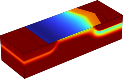
Field-effect transistors (FETs) exhibit favourable characteristics for biological and chemical sensing applications, including multi-parameter response, tunable sensitivity, and inherent amplification [1], [2]. As sensors, FETs employ their gate or active channel as a sensing area, where exposure to a biological or chemical target analyte results in a measurable threshold voltage shift or change in drain current. Various FET-based sensor configurations have been developed from the conventional metal-oxide-semiconductor FET (MOSFET) structure, enabling the deposition of various sensing materials as its conductive channel or top gate [1], [3], [4]. A critical metric for assessing the sensitivity of FET-based sensors is their transconductance. Different approaches to improve MOSFET transconductance while minimizing size include planar length scaling, width folding and stacking in three-dimensional space [1], [5], [6]. This study presents a unique approach whereby different planar gate topologies are modeled and compared against the conventional rectangular MOSFET structure. The unconventional chevron-shape and annular ring FET topologies presented in this study take advantage of angles in their geometry to increase the electric field strength, thus increasing the FET’s transconductance. These designs have not been studied for sensing applications or analyzed using finite element analysis (FEA). This study leverages the Semiconductor module in COMSOL Multiphysics® 6.2 to evaluate the unique topologies by its electric field distribution, current density, and output characteristics. 3D models created in this study reference the conventional 2D rectangular representation of a MOSFET from the application library example, DC Characteristics of a MOS Transistor. Moreover, the FETs are designed with the same gate width-to-length dimensions for fair comparison. The FET models use silicon with its relevant semiconductor material properties. COMSOL’s built-in Semiconductor physics equations for Fermi-Dirac statistics and Shockley-Read-Hall continuity model were implemented to simulate the distribution of charge carriers, and trap-assisted recombination processes, respectively. Doping profiles apply analytical and user-defined geometric doping models to represent the complex geometries. The MOSFETs' source, drain, and body terminals are treated as ohmic contacts, and the top gate is assigned as a thin insulator gate. Control of the channel's conductivity involves applying voltage to both the top gate and the drain terminals to enable current flow. All remaining boundaries of the FETs are insulated. For efficient analytical computation, the model is discretized using a swept meshing technique, which establishes mapped distributions that are more densely defined near the junctions to reflect variations in impurity doping concentration. A semiconductor equilibrium study is used to generate initial conditions for computing the output characteristics of the device. The outcome of this study is to demonstrate that incorporating angled terminals within a MOSFET structure of the same footprint enhances the electric field density, current, and consequently, the transconductance of the MOSFET compared to the conventional rectangular topology.


