了解多物理场仿真在基础研究和产品设计中的应用
各个行业的工程师和科研人员都在使用多物理场仿真来研发创新的产品设计和流程。他们在 COMSOL 用户年会上展示了丰富的技术论文和演示文稿,您可以从他们的研究成果中寻找灵感。
使用左侧【快速搜索】工具查找您感兴趣的研究,或按照应用领域进行筛选。
查看 COMSOL 用户年会 2026 论文
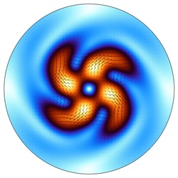
Optical tweezers enable the non-contact manipulation of micro- and nanoparticles through momentum exchange ... 扩展阅读
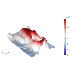
Optical tweezers enable the non-contact trapping and manipulation of micro- and nanoparticles using highly ... 扩展阅读

Silicon photonic devices feature a high degree of integration and strong optical field confinement. However, ... 扩展阅读
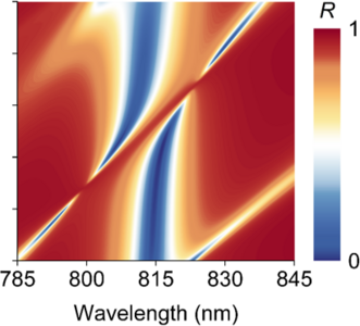
Efficient operations of hot-electron photodetectors (HE PDs) require strong energy deposition in metals ... 扩展阅读
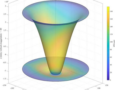
Direct wafer bonding is a key process for advanced 3D integration, in which the propagation of the bonding ... 扩展阅读

本文以n-on-p型512×1线阵 HgCdTe 探测器为例,构建二维半导体器件仿真模型,模拟了1064 nm、20 ns脉冲激光在不同功率密度范围内的载流子分布与内建电场演化过程 ... 扩展阅读

本研究利用COMSOL Multiphysics(6.4版)对TiO2/β-Ga2O3/Pd异质结进行了多物理场仿真,旨在验证并解释该高性能光电探测器背后的物理增强机制。仿真工作主要涵盖两个核心方面:首先 ... 扩展阅读

半导体激光器在高功率运行过程中会产生显著废热,阵列内部非均匀发热及微流道局部堵塞易引起结温升高和温度分布不均,并进一步造成器件中心波长的热致漂移。为研究非均匀热负载及冷却异常对半导体激光器阵列热性能的影响 ... 扩展阅读