硅表面的氩离子溅射仿真
Application ID: 140971
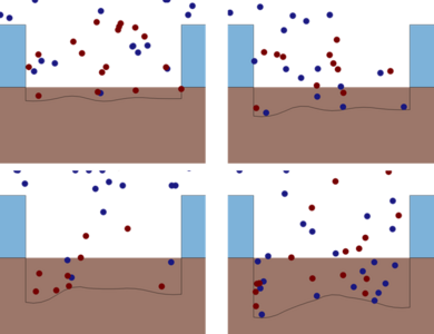
离子束刻蚀是半导体制造、材料科学和微机电系统 (MEMS) 领域不可或缺的核心工艺。为深入剖析这一复杂物理过程,本概念验证模型使用带电粒子追踪 接口,精确模拟了硅表面的氩离子溅射过程,并采用变形几何 接口捕捉和显示由溅射效应驱动的表面形貌演化过程,为工艺机理分析提供直观、可靠的仿真依据。
有关本模型的详细信息,请参阅随附的博客文章:模拟硅表面的氩离子溅射。
案例中展示的此类问题通常可通过以下产品建模:
您可能需要以下相关模块才能创建并运行这个模型,包括:
建模所需的 COMSOL® 产品组合取决于多种因素,包括边界条件、材料属性、物理场接口及零件库,等等。不同模块可能具有相同的特定功能,详情可以查阅技术规格表,推荐您通过免费的试用许可证来确定满足您的建模需求的正确产品组合。如有任何疑问,欢迎咨询 COMSOL 销售和技术支持团队,我们会为您提供满意的答复。