Evaluation of Low-Cycle-Fatigue Life of Solder Joints in Surface Mounting Power Devices by Finite Element Modeling
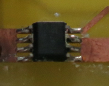
The reliability of solder joints [1,2] is one of the key factors in the determination of the reliability of the high power density electronic converters, being the solder joints both the mechanical, the electrical, and often the thermal connections between the electronic component and the board in which the component is placed. The main mechanism by which solder joints are damaged is thermal cycling and, in particular, thermo-mechanical stress-strain distribution, which arises from the different thermal expansion coefficients of adjacent materials [3]. The damaging process of solder joints, which falls in the mechanical fatigue behavior of materials, is a Low-Cycle-Fatigue (LCF) process [4] in which the soldering alloy is stressed up into the plasticization area. The simplest law which accounts for LCF-induced degradation is the Coffin-Manson law, or the extended Basquin-Coffin-Manson law which accounts for High-Cycle-Fatigue (HCF) as well [5]. Creep [6] is another important factor that contributes to the solder joint damage and has been added to the Coffin-Manson law. Here, we developed a FE model which describes the thermo-mechanical behavior of solder joints of high power density surface mounting devices (SMD), such as those used in low-medium size DC/DC converters for power supplies, both for power MOSFETs and their drivers. We used, as a case study, a power MOSFET in SO-8 package mounted on a small FR4 board (Figure 1). Thanks to their small size and the capability of handling high power densities, these devices are attractive for designing compact power supplies in which a high-power density is required. A model able to make predictions about the component operating life is mandatory in converter design. The aim of this work is to use the FEA to build a thermo-mechanical model of a power transistor subjected to thermal cycles to obtain indications about the fatigue life of the solder joints. A blow-up of the tetrahedral mesh is shown in Figure 2. The model was run at different dissipation power levels: 0.3 W, 0.4 W, 0.5 W, and 0.6 W. The purpose is to localize the most stressed solder joint in several operating conditions and the most stressed surface on that solder joint. The maximum temperature reached by the solder joints are 67 °C, 81°C, 95 °C, and 110 °C, respectively. Clearly, these are representative of an accelerated life test. From each simulation case, the algorithm presented in the previous section has been applied, and some considerations follow: (i) the solder joints 1, 2, 3 and 4 are always the most stressed; this is reasonable, being those the pins connected to the Drain terminal, with 1 and 4 being the most stressed among this set; they can move more freely than the others, and thus they are more prone to be strained. Figure 3 shows the normalized Von Mises stress per pin; (ii) the most stressed surface on pin 1 is the lateral surface (the most external one), as shown in Figure 4. Therefore, the stress-strain state on this surface will be investigated.

下载
- delmonte_poster.pdf - 0.3MB
- delmonte_paper.pdf - 1.31MB
- delmonte_abstract.pdf - 0.09MB


