Improving Convergence of Semiconductor Models
When using the COMSOL Multiphysics® software with the add-on Semiconductor Module to simulate semiconductor devices, the Semiconductor interface enables you to make assumptions to simplify the solution process by reducing the nonlinearity of your model. However, even after such assumptions are made, the governing equations in the Semiconductor interface, and consequently your model equations, are still highly nonlinear. Such nonlinearity can lead to slow convergence or difficulty converging when the model is being computed. In this article, we will outline different approaches that you can use to help improve the convergence when computing semiconductor models.
Background
The Semiconductor interface simulates semiconductor devices by solving Poisson's equation for the electrostatics and the drift–diffusion equations for electrons and holes transport under the influence of electric fields and concentration gradients in a semiconductor material. It also has capabilities for coupling with device-level models (via the Electrical Circuit interface).
The Electrical Circuit interface can be used to connect the semiconductor device with an external circuit that may include passive and active elements. The interface also has a SPICE import feature to make it easy to define the external circuit.
The governing equations in the Semiconductor interface are highly nonlinear even though several assumptions are made, as detailed under the User's Guide for the Semiconductor Module, in chapters "What Can the Semiconductor Module Do" and "Physics for Semiconductor Modeling". Different formulations, namely finite element method (FEM)-based and finite volume method (FVM)-based formulations, are used for different conditions, and there are advantages as well as considerations for using either approach. Regardless of the formulation used, it is advantageous to learn the techniques that help with the solver convergence for semiconductor models. In the following sections, we will discuss various aspects of semiconductor modeling techniques. These will include discretization formulations, meshing, the continuation solver, study types, and solver settings.
Discretization Formulations
The finite volume formulation is the default discretization for the Semiconductor interface and inherently ensures local current conservation. It is known for its stability and robustness in handling nonlinearity and providing good accuracy for problems with discontinuities or localized features. It usually provides the most accurate result for the current density of the charge carriers. Although, in some cases, using an alternative discretization formulation can make your model more computationally efficient. However, this should only be done with a thorough theoretical understanding.
The finite element formulation, which most of the physics interfaces in COMSOL Multiphysics® are based on, allows for the process of creating couplings between the Semiconductor interface and other physics interfaces to be more straightforward and efficient. (Although, FEM-based formulations are much less frequently used in semiconductor physics modeling compared to the FVM formulation.) One can differentiate variables using the d operator directly, which is not available in the finite volume formulation. It typically solves faster than the finite volume formulation and is more flexible in mesh generation. Using a linear shape function, for example, requires fewer degrees of freedom and speeds up the computation.
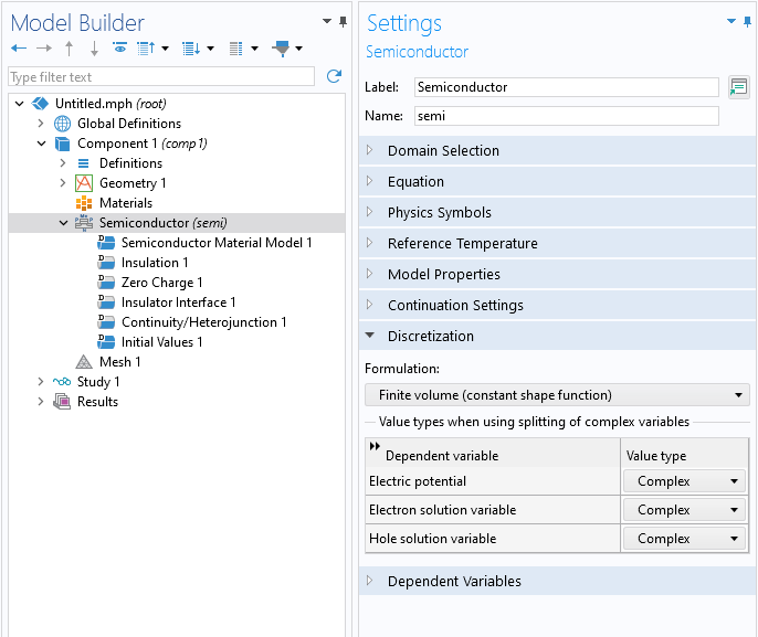 The COMSOL Multiphysics UI showing the Model Builder with the Semiconductor interface selected and the corresponding Settings window with the Discretization section expanded, showing the dependent variables and their value type.
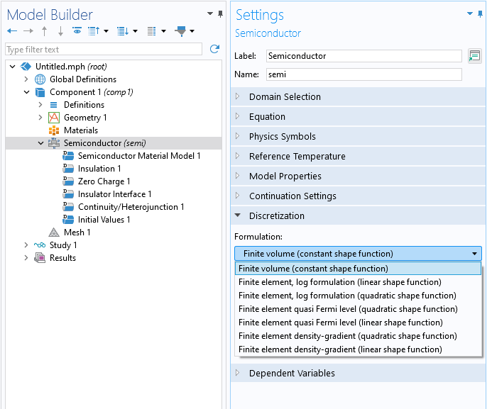 The COMSOL Multiphysics UI showing the Model Builder with the Semiconductor interface selected and the corresponding Settings window showing the settings options in the Formulation drop-down menu.
For the logarithmic finite element formulation, dependent variables are defined as the natural logarithm of the electron and hole number densities. In version 6.2 of COMSOL Multiphysics®, significant improvements have been made to the stability, accuracy, and efficiency of finite element formulations, including the log formulation. It specifically solves faster than the finite volume method and is more adaptable for different types of the mesh (which will be discussed later in this article). As a result, the majority of library models in the Semiconductor interface can now be solved more efficiently using finite element formulations, namely the Bipolar Transistor, 3D Analysis of a Bipolar Transistor, and Thermal Analysis of a Bipolar Transistor models. These models showcase the advantages of the finite element discretization with log formulation where the models not only are easier to set up but also demonstrate more efficient solutions.
The quasi-Fermi level formulation introduces quasi-Fermi levels for electrons and holes as dependent variables to simplify the solution of the drift–diffusion equations and reduce computational complexity. It can be suitable for systems with wide band gaps or at very low temperatures, where the transport of charge carriers is typically highly sensitive to the shape of potential barriers (such as tunneling effects across the barriers). The default finite volume formulation, due to its discontinuous treatment of variables across the mesh interfaces, would require a much finer mesh near the barriers for those systems. See: Heterojunction Tunneling.
The density-gradient formulation extends the quasi-Fermi level formulation and provides a computationally efficient method to include the effect of quantum confinement by implementing the effective mass approximation in the conventional drift–diffusion equations. See: Nanowire MOSFET.
General Considerations
Good Initial Conditions and Continuation Solver
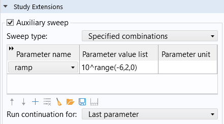
The nonlinearities in the governing equations solved by the Semiconductor interface arise due to many factors: for instance, the exponential relationship between the carrier concentration and the energy bands; the nonuniform distribution of carrier concentrations and doping profiles; carrier recombination and generation processes; electric field-dependent quantities; and many other factors that contribute to the nonlinear behaviors of semiconductor materials. Good initial values typically provide a good start for solving nonlinear problems. Within FVM formulation, the Semiconductor Equilibrium study can often provide a good initial condition for subsequent ramping up of applied voltages. In FEM formulation, smooth initial conditions are beneficial as well. While this is not crucial for Poisson’s equation, it is important for transport equations due to significant electron and hole density gradients. Hence, it is advisable to start with values near the final results and maintain the default Intrinsic initial condition. The default initial values in the Semiconductor interface provide good and rough guesses for the carrier concentration in the absence of applied voltages or currents. When you solve stationary models, it is recommended to ramp up the voltages or currents to the operating values. This can be achieved by defining the applied voltages or currents as parameters and then enabling an auxiliary sweep where the values are gradually incremented starting from zero. Ramping the bias voltage is also the method for obtaining the I-V curve for understanding the electrical behavior of the device. The sweep can be implemented in the Settings window of a study step node, such as in the Stationary study step (pictured below).
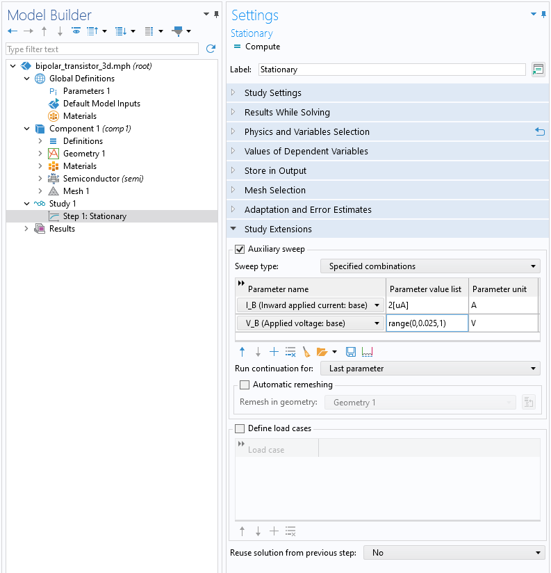
An auxiliary sweep (for parameters defining a voltage and current for a model) is enabled under the Stationary study step.
Note that you need to choose Last parameter from the Run continuation for list. This setting specifies the parameter on which the continuation solver should be applied. When performing multiple sweeps with the sweep type set as All combinations, it is recommended to set the Reuse solution from previous step setting to Auto.
The initial values can also be the solution from another study by adjusting the settings in the Values of Dependent Variables section of the study step. To achieve this, choose User controlled under Initial values of variables solved for, then choose Solution for the Method option, and then choose the best solution from the Study list, as shown below.
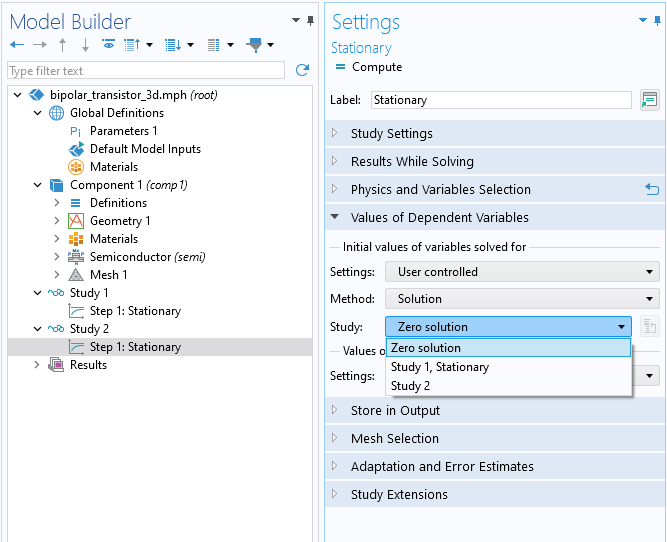
Settings for the Values of Dependent Variables section of the Stationary study step, through which you can select the solution from another study to serve as the starting point of the analysis.
Besides incrementally increasing currents and voltages, the continuation solver also allows for gradually introducing nonlinear contributions to the governing equations — something that is especially useful in highly nonlinear problems. This capability is enabled through the Continuation Settings section, which is available for several physics feature nodes, including the nodes for doping, trap density, and heterojunction.
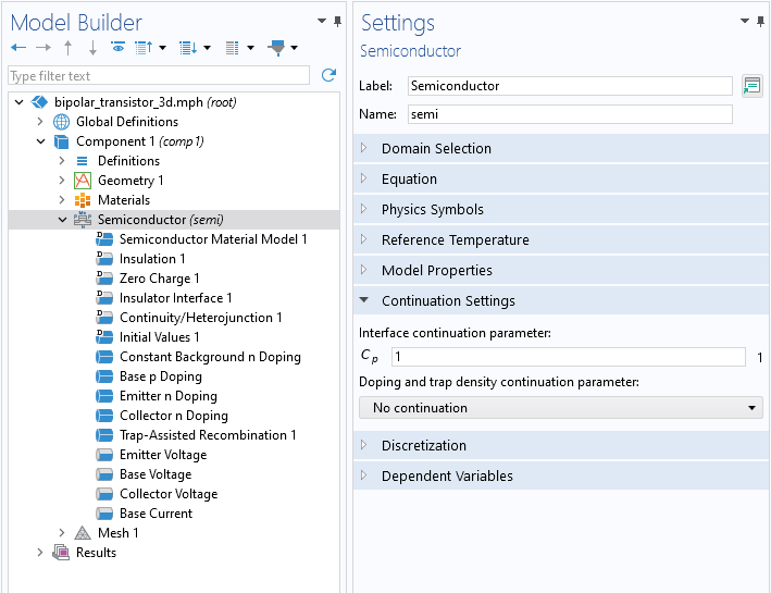 The Model Builder with the Semiconductor interface selected and the corresponding Settings window showing the Continuation Settings section.
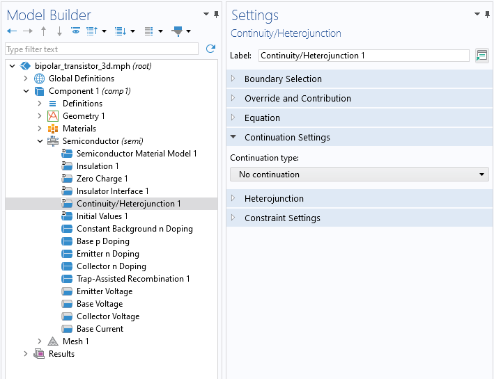 The Model Builder with the Continuity/Heterojunction node selected and the corresponding Settings window showing the Continuation Settings section.
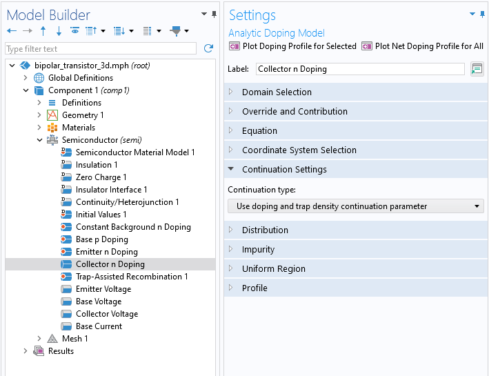 The Model Builder with the Collector n Doping node selected and the corresponding Settings window showing the Continuation Settings section.
To enable the continuation solver, a parameter should be set in the Continuation parameter section and ramped from 0 to 1, which determines the scaling of the equation contribution and slowly increases the nonlinear contribution to the system. When choosing the Use interface continuation parameter option, the continuation is linked to the value of the interface-level continuation parameter specified in the Continuation Settings section of the Semiconductor interface settings window (pictured above, to the left). This allows several features (the equation scaling, doping, trap density, and selected nonlinear contributions) to be ramped up together.
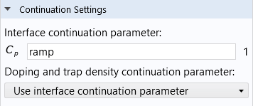
The interface continuation parameter is set under the Continuation Settings section in the Semiconductor interface node.
The auxiliary sweep for the interface continuation parameter.
When the dopant concentration is ramped up and the finite volume method is the selected discretization formulation, it is recommended to start from a small value (for instance, 1e-6) rather than zero since the continuation solver does not handle the transition from no doping to finite doping for this numerical method. In addition to ramping the dopant concentration, the following elements can be ramped up by the same method: the trap density; bias voltages and currents; and other properties, such as field-dependent mobility as well as recombination and generation rates.
When the continuation solver is enabled and the carrier mobility is field dependent, it can be beneficial to configure the Predictor in the continuation solver as Linear. This setting accelerates the voltage sweep by employing a linear extrapolation method to estimate the initial approximation for the next parameter being swept. By default, the Constant option uses the current solution as the starting estimation. This approach is more conservative and generally suitable in most cases.
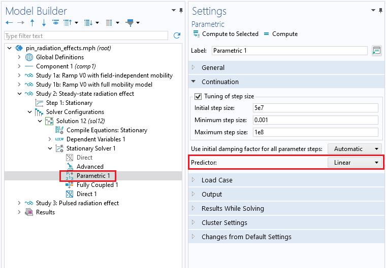
The Predictor setting is set as Linear in the Parametric node of the solver configurations.
There are two special cases where good initial values are achieved by certain methods:
- In the case of a heterojunction condition, use the solution of the continuous quasi-Fermi levels setting as the initial value for the Thermionic emission setting. (See: Heterojunction 1D.)
- In the case of a current-driven bias, use the solution of a voltage-driven bias as the initial value. (See: InGaN/AlGaN Double Heterostructure LED.)
For some multiphysics applications, it is good practice to solve one physics first and then solve the fully coupled model in the following study step. For instance, when modeling optoelectronic devices, the wave optics physics can be solved first and then the multiphysics coupling between semiconductor and wave optics can be solved in the following study step, where the solver automatically uses the first study step's solution as the initial values of the second study step.
We recommend the following resources to learn more about running the continuation solver:
- Improving Convergence of Nonlinear Stationary Models
- Load Ramping of Nonlinear Problems
- Nonlinearity Ramping for Improving Convergence of Nonlinear Problems
Meshing
It is essential to ensure that there are no large changes in the results as the meshing for your semiconductor model is refined. This description is sometimes referred to as mesh independence. To see different strategies for performing mesh refinement analysis, see Performing a Mesh Refinement Study.
The most optimal meshing for discretizing your model will depend on the formulation of the semiconductor equations, e.g., the finite element formulation or finite volume formulation. COMSOL Multiphysics® will automatically refine the mesh based on the physics you are simulating as well as the physics feature nodes used to define the physics in your model.
It is crucial to create finer mesh in the vicinity of junctions for both finite elements and finite volumes. For instance, near a thin insulator gate, the mesh element size needs to resolve the oxide thickness. This can be done by creating a mesh-controlled region in the geometry for the oxide thickness. (See the MOSCAP 1D tutorial model.) You can also use the mapped mesh technique (for 2D) and the swept mesh technique (for 3D) to generate predefined mesh distribution for a local refinement. (See the 3D Trench Gate IGBT tutorial model.) Another case is near a Schottky contact, where the depletion region needs to be resolved. Besides gate boundaries, the regions near the junctions also include heterojunctions, doping profile edges, and trap-assisted surfaces.
Another option for mesh refinement is to use the Adaptation functionality in the study settings, which refines the mesh in the geometry regions where the error in the solution is largest. The Semiconductor Module also provides a predefined study type, the Semiconductor Initialization study, which is used to adaptively refine the mesh based on the gradient of the impurity doping concentration. It solves a nonphysical equation that causes the mesh to be refined in regions where the gradient of the doping is large.
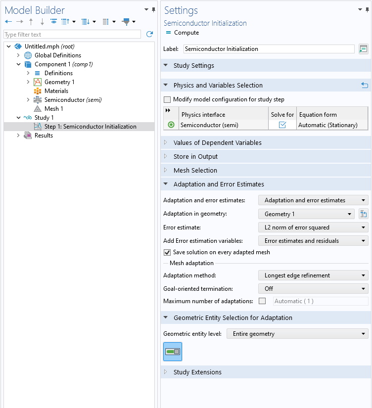
The Semiconductor Initialization study step with the Adaptation and Error Estimates settings expanded.
We recommend the following resources to learn more about meshing in general as well as for semiconductor modeling:
- An overview of the meshing workflow, fundamentals, and best practices for how to build meshes
- A video tutorial on meshing practices for modeling semiconductor devices
- An introduction to meshing operations and parameters
- An introduction to how swept meshing can improve your mesh
- An introduction to building swept meshes
FVM: Approaches for Improving Convergence
Meshing
In the finite volume formulation, triangular or rectangular mesh elements work best for 2D models. As for 3D models, creating a boundary mesh of triangular or rectangular elements and then using a swept mesh is most optimal. (For finite volumes in 3D, tetrahedral elements are not currently supported.) You can build a triangular mesh in the plane of a wafer surface and use a swept mesh to extend that meshing into the 3D wafer domain. This implementation can be especially important for certain applications, such as for gate contacts. You can see this implementation in the image below, which shows meshing gates for a 3D model using finite volumes.
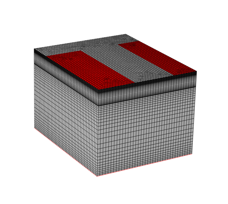
An example of a suitable mesh for a gate contact in 3D, which is generated using a swept mesh. The sweep direction for this swept mesh in the 3D bipolar transistor tutorial model is perpendicular to the gate, in the z direction, using a geometric sequence with an element ratio of 0.25. The emitter is the leftmost red section, the base is the rightmost red section, and the collector is the bottommost red section (it is thin; appearing as a line along the bottom perimeter). The mesh is refined where the Gaussian profile of doping drops off between the contacts.
Equilibrium Study
The Semiconductor Module offers a predefined study type, the Semiconductor Equilibrium study, which can provide a good initial condition for the ramping of applied voltages. It computes the semiconductor solution, assuming the system is under thermal equilibrium. When the charge carriers are in thermal equilibrium, only Poisson’s equation is solved (while still taking into account the space charge density from the charge carriers and the ionized dopants). This provides the most efficient solution for systems known to be in equilibrium, as well as an option to generate the initial condition for solving nonequilibrium models. Note that all metal contacts attached to the same Semiconductor Material Model domain are biased at a common voltage, with the default being zero, as dictated by the equilibrium condition.
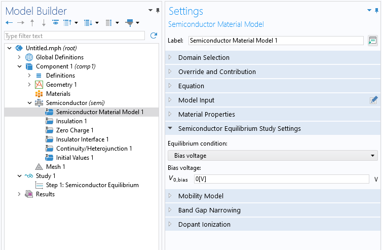
Bias voltage for the Semiconductor Equilibrium study.
To learn more about the techniques mentioned here, we recommend the following resources:
- The nanowire traps tutorial model
- Uses the continuation solver (through the auxiliary sweep and the continuation parameter, as discussed earlier in this article) for ramping nonlinear contributions to the model
- The heterojunction 1D tutorial model
- Shows some standard approaches for reaching convergence for stationary (steady-state) studies
- The forward recovery of a PIN diode and reverse recovery of a PIN diode tutorial models
- Show using the equilibrium or stationary solution for the model in the Time Dependent study step as the initial condition
Solver Tolerance
The solver tolerance plays a crucial role in numerical calculations. Choosing an appropriate solver tolerance is essential for balancing computational efficiency and accuracy. COMSOL Multiphysics® typically defines the solver tolerance by default based on the problem's characteristics, desired accuracy, and computational constraints. For some cases of semiconductor modeling, such as modeling minority carrier devices, tightening the solver tolerance might be necessary to ensure the solution converged within sufficient accuracy. If the carrier concentrations in the results turn out to be negative, you should tighten the solver tolerance from 1e-6 (default) to 1e-9 or lower to solve this nonphysical issue.
The Heterojunction 1D tutorial model demonstrates the technique of tightening the solver tolerance to help convergence and improve accuracy for stationary (steady-state) studies.
The solver tolerance for a stationary study can be adjusted in the Stationary Solver node of the Solver Configurations node. The Time-Dependent Solver has both relative and absolute tolerance settings. The Relative tolerance setting is available in the Time Dependent study step. The absolute tolerance is set in the Time-Dependent Solver node under Solver Configurations.
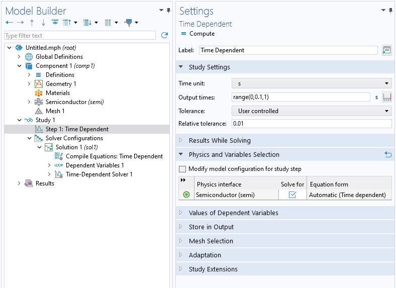
The Relative tolerance setting in the Time Dependent study step.
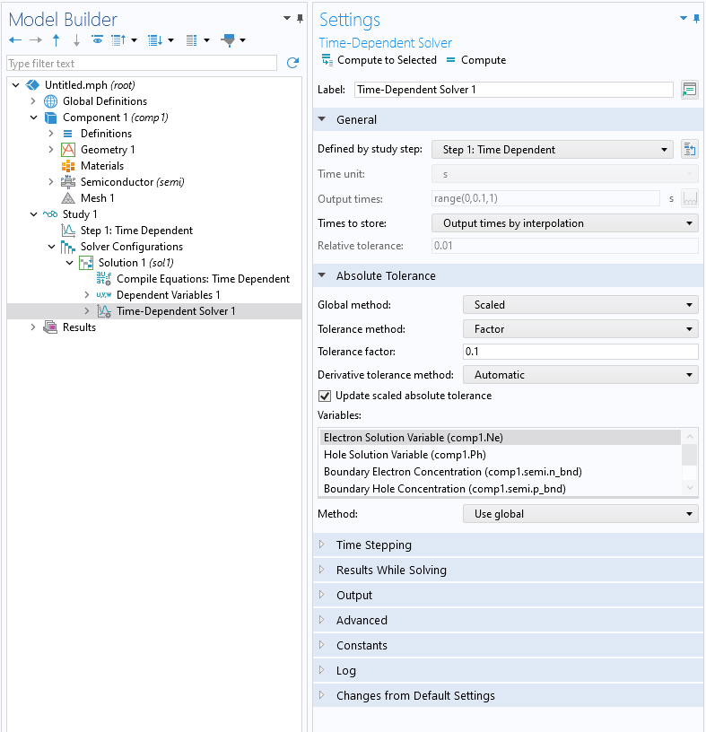
The Absolute Tolerance section settings in the Time Dependent Solver node.
In addition to the solver tolerance, there are some other solver settings that can be adjusted to help solvers converge. These include using the Fully Coupled and Direct solvers, increasing the maximum number of iterations, and setting the scaling of dependent variables to Initial value based.
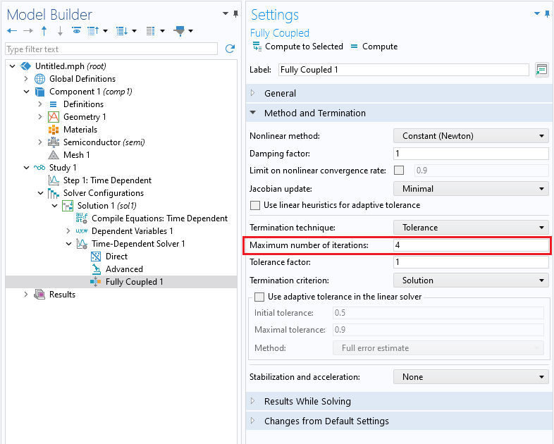
Increasing the maximum number of iterations.
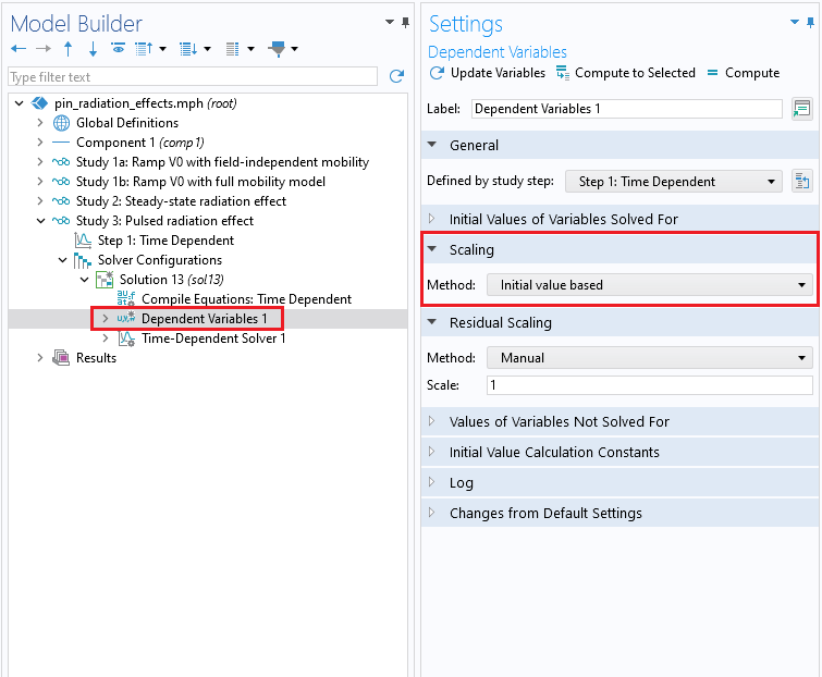
Scaling of dependent variables.
FEM: Approaches for Improving Convergence
Meshing
In the finite element method, both the log and linear formulation work well with all types of mesh elements. For instance, solving a 3D bipolar transistor model with the finite volume formulation would typically take a day. However, with the improved finite element discretization with log formulation in version 6.2, the model is solved in 15 minutes on a standard PC. This is mainly due to several capabilities of log formulation in finite element discretization: First, unlike the finite volume formulation, the 3D finite element formulation does not necessitate a swept mesh. Second, the finite-element log formulation with linear shape function significantly reduces the degree of freedom required for tetrahedral meshes in 3D.
It is important to evaluate the dependence of the global current conservation on the mesh for the indication of the overall accuracy of the model solution. If current conservation is still poor after running mesh refinement analysis, then tightening the solver tolerances may be required, which is discussed further above in this article.
Concluding Remarks
Here, we have provided general guidelines that you can use to improve the convergence of semiconductor models. We discussed the impact of various aspects of semiconductor modeling techniques including meshing, discretization formulations, continuation solver, and solver settings. Among all, it is recommended to ramp up excitations, that is, incrementally increase the voltages/currents to their operational values. Another options is to use the continuation solver, which allows for gradually introducing nonlinear contributions to the governing equations, such as doping and trap densities. These can help ensure a smoother transition to the operating values, which can lead to more accurate and stable solutions in your models.
Further Learning
To learn more about the techniques introduced here and discover new ones, check out the following resources:
- Improving Convergence of Nonlinear Stationary Models
- Improving Convergence of Nonlinear Time-Dependent Models
- Finite Element Mesh Refinement
- Performing a Mesh Refinement Study
- Using Swept Meshes for Model Geometries
请提交与此页面相关的反馈,或点击此处联系技术支持。