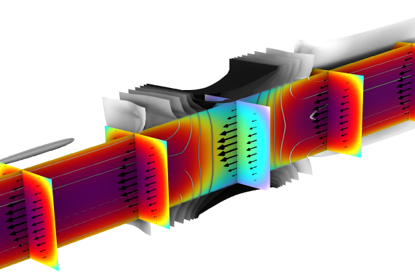
Built-in Multiphysics Couplings for Semiconductor Devices
In Part 6 of this course on semiconductor modeling, we discuss some additional multiphysics couplings. The optoelectronics coupling between the Semiconductor and electromagnetic waves interfaces take place through the Optical Transitions feature, which introduces a stimulated generation term on domains within the Semiconductor interface and takes spontaneous emission into account in direct-band-gap materials. This functionality is based on the frequency domain and beam envelopes interfaces within the Wave Optics Module. The effect of the light absorption or emission is accounted for by a change in the complex permittivity or refractive index. We then demonstrate how to use the optoelectronics coupling when modeling both light emitting diodes (LEDs) and photodiodes. The electric circuit coupling between the Semiconductor and Electric Circuit interfaces is used to connect a semiconductor device in the circuit to the semiconductor interface via a metal contact, thin insulator gate, terminal, floating potential, or floating gate.
Discussion and Demo: Optoelectronics
We begin with taking a look at the built-in optoelectronics coupling that is designed for modeling LEDs, photodiode and optical sensors. First, we will look at the optical transitions using only the Semiconductor interface and continue with how you can couple that with the Wave Optics interface. Using the Optical Transitions feature in the Semiconductor Module, you can introduce a spontaneous emission and stimulated absorption and emission. We will use the gallium nitride (GaN) LED tutorial model to demonstrate some of the key features of modeling optoelectronics, including spontaneous optical emission, Auger recombination, and trap assisted recombination. Here, you will see the full model build from start to finish and learn how current-driven models can be solved by generating initial conditions from voltage-driven studies.
Demo: Photodiode
We continue with expanding on what we learned in the the previous video by including stimulation effects with the GaAs PIN Photodiode tutorial model. Photodiodes are semiconductor devices that convert incident light into a current. Incident photons with energy larger than the band gap can be absorbed by interacting with an electron in the valence band and promoting it across the band gap in the conduction band. When absorbed, the photon creates a hole in the valence band and an electron in the conduction band. The extra photons generate carriers that can be separated and collected, resulting in a current from the device terminals. The doping and electrical contacts are defined by the Semiconductor interface while the incident electromagnetic radiation is defined by the Electromagnetics Waves, Frequency Domain interface. The absorption is computed using a direct band-gap model, which assumes parabolic bands and both spontaneous and stimulated emission are computed using the spontaneous lifetime of electron-hole pairs with the material to calculate the interaction strength between carriers in the conduction and valence bands. Here, you will see the model building process from start to finish.
Discussion and Demo: Electrical Circuit Couplings
Metal contacts in the Semiconductor Module can be driven with an external circuit using the Electrical Circuit interface. The Electrical Circuit interface is used for creating lumped systems to model currents and voltages in circuits, which is helpful when modeling typical voltage and current sources, resistors, capacitors and other semiconductor devices. These models can also connect to distributed field models in 2D and 3D. Circuit topologies can be imported or exported in the SPICE netlist format. We will compare a full device led simulation with a lumped circuit model to simulate a half-wave rectifier using the p-n Diode Circuit tutorial model. The p-n diode is often used as a rectifier to convert alternating currents (AC) to direct currents (DC) by blocking either the positive or negative half of the AC wave. In this video, we will introduce the model and talk you through the basic features you will need to complete the building it.
请提交与此页面相关的反馈,或点击此处联系技术支持。


