Wafer Vacuum Adsorption by a Grooved Chuck
Application ID: 152121
In semiconductor manufacturing, vacuum chucks are used to rapidly and contamination-free adsorb and secure wafers before processes such as transfer, lithography, and inspection. Traditional empirical design makes it difficult to quantify the effects of groove shape, size, distribution, and initial wafer warpage on adsorption performance.
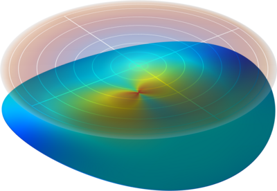
This example presents a coupled fluid-structure-contact model that captures the interaction between the pressure distribution in the chuck grooves and wafer deformation during adsorption. The model provides quantitative insight into the chucking mechanism and serves as a basis for optimizing groove design.
案例中展示的此类问题通常可通过以下产品建模:
您可能需要以下相关模块才能创建并运行这个模型,包括:
建模所需的 COMSOL® 产品组合取决于多种因素,包括边界条件、材料属性、物理场接口及零件库,等等。不同模块可能具有相同的特定功能,详情可以查阅技术规格表,推荐您通过免费的试用许可证来确定满足您的建模需求的正确产品组合。如有任何疑问,欢迎咨询 COMSOL 销售和技术支持团队,我们会为您提供满意的答复。